

City in Jiangsu turning more lab breakthroughs into global competitive edge
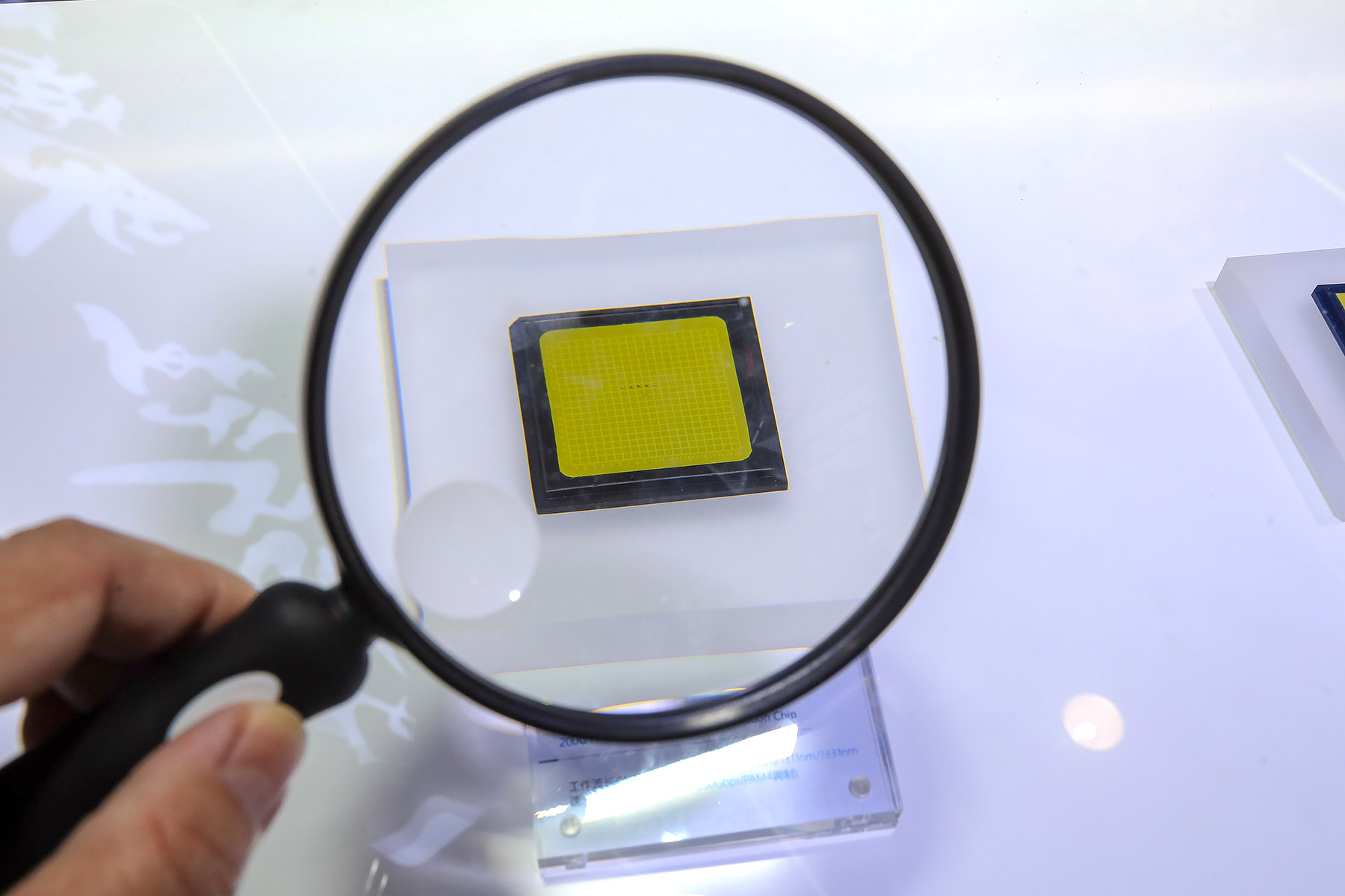
In a spotless factory floor in Suzhou, eastern China's Jiangsu province, invisible beams of light are becoming the new fuel for the artificial intelligence revolution.
Behind layers of protective glass inside the cleanroom of Suzhou Everbright Photonics Co Ltd, machines operate around the clock, producing tiny optical chips that are increasingly critical to the AI boom.
The company is producing 800G (gigabits per second, or Gbps) and 1.6T (terabits per second, or Tbps) high-speed optical communication chips designed to shuttle enormous volumes of data between servers as companies around the world race to build faster and more powerful computing systems.
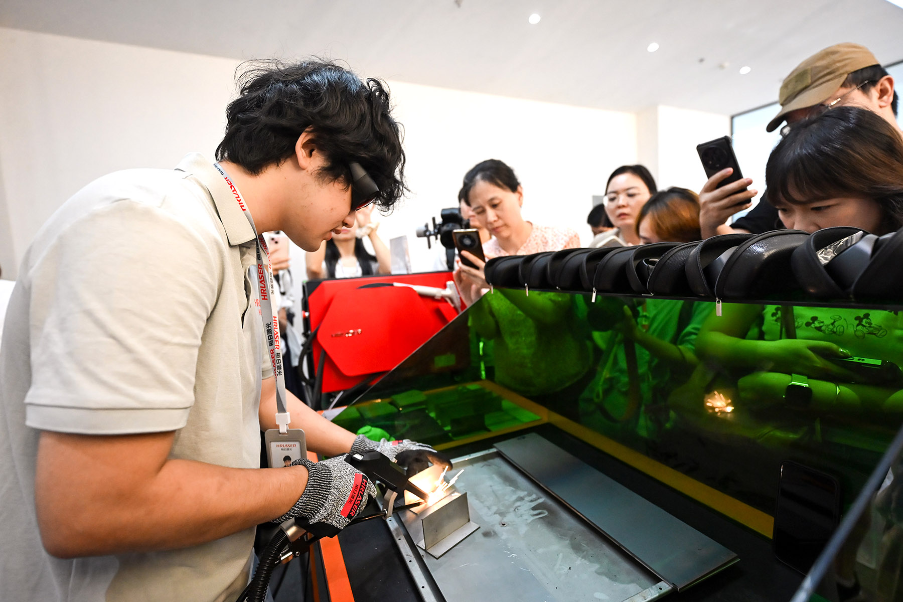
A few kilometers away, Maxphotonics is pushing light to another extreme. At its industrial park, the company has developed what it calls the world's first 160-kilowatt ultra-high power fiber laser, powerful enough to cut through exceptionally thick industrial materials.
READ MORE: AI reshaping China's workforce
Together, more than 350 photonics and related companies capture a broader transformation underway in Suzhou: a manufacturing powerhouse better known for electronics and industrial production is betting heavily on photonics as a new engine of growth.
As the AI boom sends demand for computing power soaring and manufacturers seek more advanced production tools, the city is building an ecosystem stretching from optical chips and silicon photonics to industrial lasers — part of China's broader push to move from manufacturing scale to technological strength.
AI may be built on algorithms and computing chips, but moving data between those chips is becoming a growing challenge. Training and running advanced AI models requires thousands, and sometimes tens of thousands, of processors to work together. The more computing power that is packed into a data center, the more information must travel between servers and clusters — quickly and without consuming prohibitive amounts of electricity.
That is putting optical communications at the center of the AI infrastructure boom.
At Everbright, 800G and 1.6T optical communication chips are in round-the-clock production, targeting the high-speed connections required by increasingly powerful computing clusters.
For Suzhou, that demand has opened a window to move into a segment of the technology supply chain where China once relied heavily on overseas suppliers.
A group of Suzhou optical communication companies recently pooled investment to begin construction of what they describe as China's first 8-inch silicon photonics chip mass-production line.
The project is designed specifically for the research, development and manufacturing of next-generation high-speed optical modules.
Silicon photonics uses semiconductor manufacturing techniques to integrate optical functions onto silicon, potentially allowing faster data transmission at lower power consumption and greater scale.
Turning that promise into mass production, however, is difficult. It requires not only chip design, but manufacturing processes, packaging, testing equipment and customers willing to validate new products.
The Suzhou production line aims to close that gap and fill a domestic void in the large-scale manufacturing of high-end silicon photonics integration.
For Everbright Chairman Min Dayong, it marks the latest chapter of a journey that began when China's photonics industry looked very different.
When Everbright arrived in Suzhou New District, or Suzhou High-tech Development Zone, in 2012, China's high-power semiconductor laser chip sector was still in its infancy.
Overseas companies dominated the market. Chinese manufacturers lagged in manufacturing yield, output power and other key capabilities, while high-end industrial and medical applications depended heavily on imported components.
Everbright faced a daunting combination of obstacles: technological barriers, expensive semiconductor equipment, scarce capital and a shortage of specialized engineers.
The company's expansion can be traced through the physical spaces it occupied. It started with a relatively small research and development facility. As it grew, it moved into its industrial park headquarters. In 2026, the ecosystem expanded again with the 1.2-billion-yuan ($177.84 million) project and its 8-inch silicon photonics production line.
"If there had been no policy support from Suzhou New District, we would not have been able to make the breakthrough from zero to one," Min said. "This is a place where we can focus on innovation."
At Maxphotonics, the power of light can be measured on an entirely different scale.
Its 160-kW ultra-high power fiber laser, which the company describes as a world first, can handle cutting at the meter scale in some applications and stably process conventional thick plates of more than 500 millimeters, according to the company.
Such systems have potential applications in heavy industries where manufacturers must cut extremely thick materials quickly and precisely.
But the headline number — 160 kW — tells only part of the story.
Behind the machine is a supply chain of laser chips, optical fibers and other components that Chinese manufacturers once struggled to produce domestically.
"Laser chips, which are among the core components, used to rely mainly on imports. Now they can be supplied locally in Suzhou," said Dang Jiantang, deputy general manager of Maxphotonics' Suzhou subsidiary.
The company has developed technologies ranging from high-power components to triple-cladding fiber solutions as it seeks greater control over its core supply chain.
For Maxphotonics, Suzhou offered something that financial incentives alone could not provide: proximity.
Suppliers are nearby. Customers are nearby. Engineers and universities are nearby. And beyond Suzhou lies the wider Yangtze River Delta, one of the world's densest manufacturing regions.
Maxphotonics settled in Suzhou's Xiangcheng district in 2018. Its local workforce has since grown from around 40 or 50 people to more than 1,900.
The company recorded revenue of 1.5 billion yuan in 2025 and invested more than 50 million yuan in R&D, equivalent to more than 3 percent of its main business revenue.
Local measures included three years of free rent for 1,000 square meters of space and talent support worth up to tens of millions of yuan, according to materials provided by the local government.
But Dang said the deeper attraction was the supply chain.
Suzhou mapped the city's photonics ecosystem, helping companies identify potential suppliers and partners. That enabled Maxphotonics to work with local chip makers on technical problems that previously depended on overseas components.
The company has since expanded into more than 60 countries and established operations in Europe and the United States, combining research capabilities elsewhere with Suzhou's manufacturing base.
It is an example of a model increasingly visible across China's advanced industries: innovation spread across regions, but anchored by dense manufacturing clusters capable of turning technology into products at scale.
Suzhou officials describe their approach to photonics with a metaphor borrowed from the industry itself: rather than flooding the sector with support, policy should work like a laser, focusing resources where they are needed.
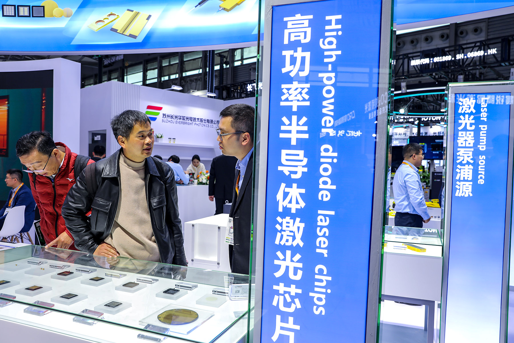
Suzhou's photonics industry has now surpassed 430 billion yuan in scale, according to Qiao Yan, deputy head of the high-tech and industrialization at the Suzhou Municipal Science and Technology Bureau.
In July, the city released plans to accelerate the development of its"10+10" key industries, placing photonics and optical manufacturing among 10 emerging sectors it wants to cultivate.
"Suzhou will focus on building a photonics innovation cluster and strive to become a core global supporting force across chips, devices and end products," Qiao said.
The challenge is that photonics does not always fit conventional economic development models.
Research costs are high. Commercialization cycles are long. Equipment can be enormously expensive. A promising company may spend years burning cash before its technology produces significant revenue.
Suzhou New District has therefore adopted different support mechanisms depending on a company's stage of development.
Startups can receive industrial space and credit. Growing companies can access R&D support and shared technology platforms. Companies entering expansion phases can tap industrial funds and application opportunities.
The district has established infrastructure including advanced compound-semiconductor and silicon-photonics platforms, allowing smaller companies to use costly equipment without having to purchase entire production systems themselves.
In 2025, it established a 1.2-billion-yuan photonics industry fund that has invested in 10 local projects.
The support extends to people as well as companies. High-end researchers can receive assistance covering housing, children's education and research funding, aimed at allowing scientists to concentrate on technical work.
And the policies change as the technology changes.
As AI computing and silicon photonics emerged as major opportunities in 2025 and 2026, Suzhou New District updated its support measures and opened a faster research and approval channel for Everbright Photonics' high-speed optical chip projects, cutting some approval processes from months to about two weeks.
For companies moving overseas, local commerce authorities have offered support for participation in international photonics exhibitions and helped companies strengthen overseas patent portfolios.
Yet perhaps the clearest explanation of Suzhou's strategy is found not in a government document, but inside Everbright Photonics' headquarters.
A dozen companies incubated along the photonics supply chain operate in the building, sharing epitaxy, packaging and testing platforms. Three have grown into certified high-tech enterprises and two into fast-growing "gazelle" companies.
The arrangement tackles a persistent problem in advanced manufacturing: an innovation is only as strong as the weakest link in the chain around it.
A chip company needs packaging. A laser producer needs optical components. A startup needs equipment to test its technology. And all of them need customers willing to put new products into real machines.
Xu Zhuqing, a researcher at the Chinese Academy of Science and Technology for Development, said the city's growth reflects a wider acceleration in China's optoelectronics sector.
ALSO READ: Suzhou encourages foreign investment, pushes for high-quality development
"Over the past two years, China has continuously made breakthroughs in key and core technologies in optoelectronic information," Xu said. "The explosive growth in demand for AI computing clusters is also driving the industry's overall expansion."
For China's photonics companies, the next test is whether technologies developed to reduce dependence on imports can compete beyond the domestic market.
Everbright Photonics said revenue from its industrial chips in China jumped more than 80 percent in 2025. It has also signed long-term agreements with companies in Germany and South Korea. Maxphotonics, meanwhile, is selling into more than 60 countries and regions.
For decades, Suzhou prospered by plugging itself into global supply chains, assembling electronics and manufacturing goods for companies around the world.
Now it is trying to move deeper into the technologies inside those products — the chips that transmit data, the lasers that shape materials and the manufacturing processes that determine whether lab breakthroughs can be produced by the millions.
Contact the writers at chengyu@chinadaily.com.cn
